03 SPI
The special function register SPI memory mapped to address 4100 enables HACK to read/write bytes from the spi flash memory chip W25Q16BV situated on iCE40HX1K-EVB. The timing diagramm for SPI communication looks like the following diagram (we use CPOL=0 and CPHA=0).

Chip specification
| IN/OUT | wire | function |
|---|---|---|
| IN | in[7:0] | byte to be sent. |
| IN | in[8] | =0 (and load=1) send byte and set CSX low |
| IN | in[8] | =1 (and load =1) pull CSX high without sending byte |
| IN | load | =1 initiates the transmission, when in[8]=0 |
| OUT | out[15] | =0 chip is busy, =0 chip is ready |
| OUT | out[7:0] | received byte (when out[15]=0) |
| OUT | CSX | chip select not |
| OUT | SDO | serial data out |
| OUT | SCK | serial clock |
| IN | SDI | serial data in |
When load=1 and in[8]=0 transmission of byte in[7:0] is initiated. CSX is goes low (and stays low even when transmission is completed). The byte is send to SDO bitwise together with 8 clock signals on SCK. At the same time the SPI receives a byte at SDI. During transmission out[15] is 1. After 16 clock cycles the transmission of one byte is completed. out[15] goes low and SPI outputs the received byte to out[7:0].
When load=1 and in[8]=1 CSX goes high without transmission of any bit.
Attention: Sampling of SDO is done at rising edge of SCK and shifting is done at falling edge of SCK.
Proposed Implementation
Use a Bit to store the state (0 = ready, 1 = busy) which is output to out[15]. Use a counter PC to count from 0 to 15. Finally we need a BitShift8L. This will be loaded with the byte in[7:0] to be send. Another Bit will sample the SDI wire when SCK=0 and shift the stored bit into the BitShift8L when SCK=1. After 8 bits are transmitted the module cleares out[15] and outputs the received byte to out[7:0].

Memory map
The special function register SPI is mapped to memory map of HACK according to:
| address | I/O device | R/W | function |
|---|---|---|---|
| 4100 | SPI | R | out[15]=1 if busy, out[7:0] received byte |
| 4100 | SPI | W | start transmittion of byte in[7:0] |
cat.asm
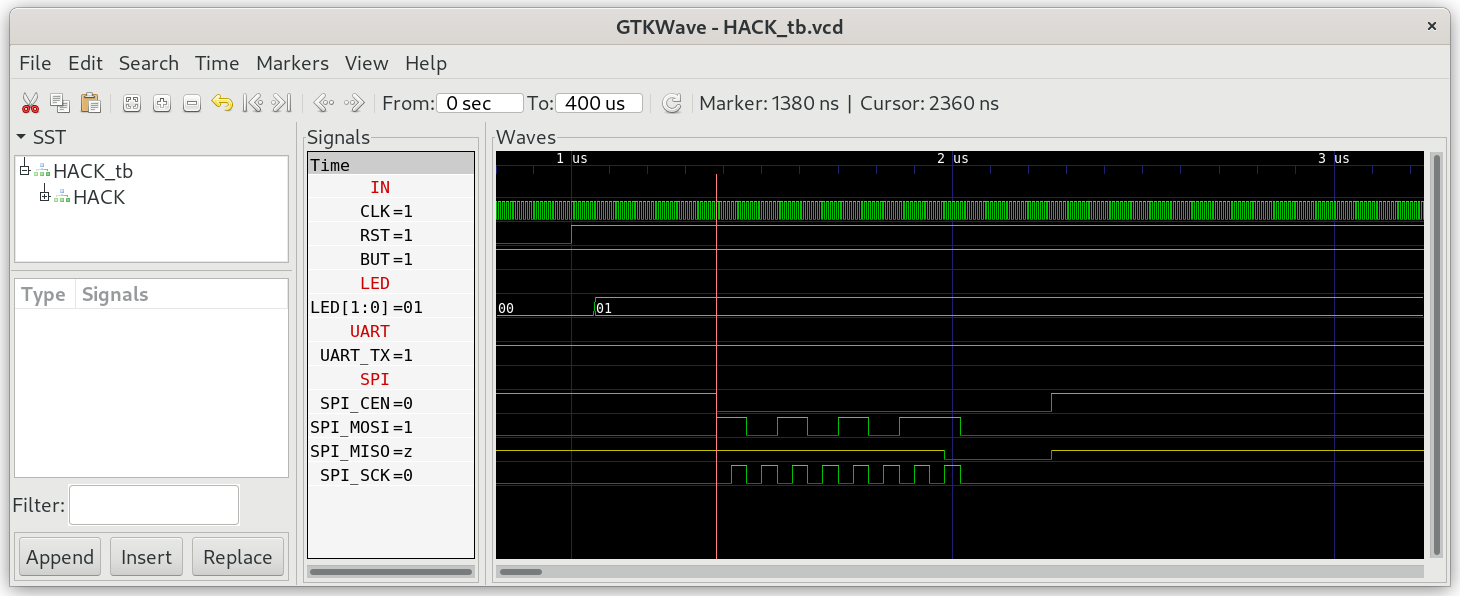
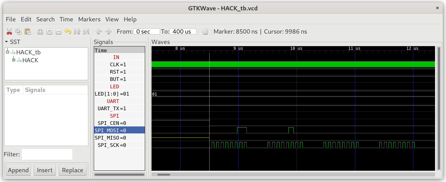
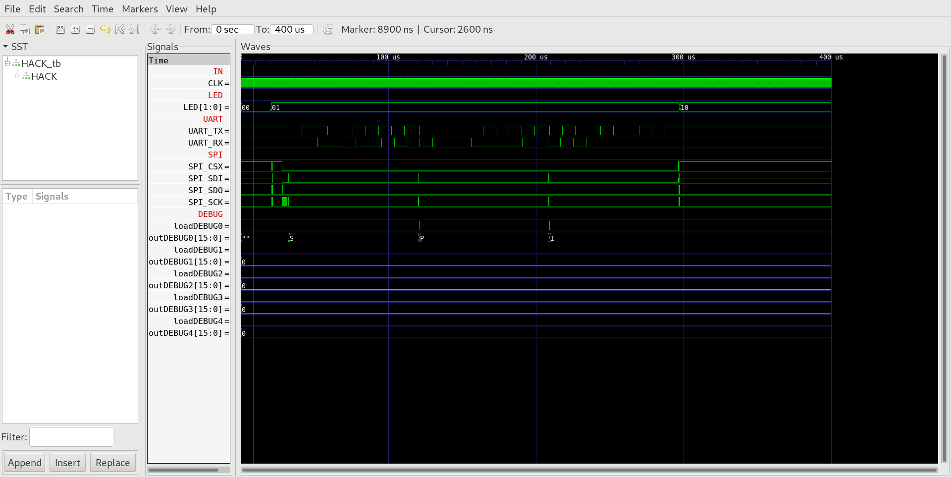
To test HACK with SPI we need a little machine language programm cat.asm, which reads 4 consecutive bytes of SPI flash memory chip W25Q16BV of iCE40HX1K-EVB, starting at address 0x040000 (256k) and sends them to UART_TX.
According to the datasheet of spi flash rom chip W25Q16BV the commands needed to read the flash rom chip are:
| command | function |
|---|---|
| 0xAB | wake up from deep power down (wait 3us) before launching next command. |
| 0x03 0x04 0x00 0x00 | read data (command 0x03) starting at address 0x040000 (256k) |
| 0xB9 | go in power down |
SPI in real hardware
The board iCE40HX1K-EVB comes with a SPI flash rom chip W25Q16BV. The chip is already connected to iCE40HX1K according iCE40HX1K-EVB.pcf (Compare with schematic iCE40HX1K_EVB.
set_io SPI_SDO 45 # iCE40-SDO
set_io SPI_SDI 46 # iCE40-SDI
set_io SPI_SCK 48 # iCE40-SCK
set_io SPI_CSX 49 # iCE40-SS_B
Project
-
Implement
SPI.vand test with testbench:$ cd 03_SPI $ apio clean $ apio sim -
Compare output
OUTof special function tregisterSPIwithCMP.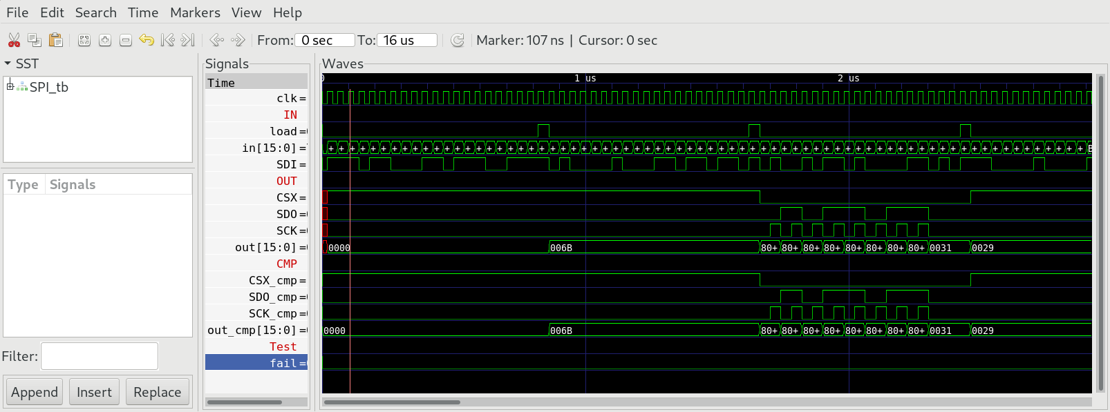
-
Add special function register
SPItoHACK.vat memory address 4100. -
Implement
cat.asmand test in simulation:$ cd 03_SPI $ make $ cd ../00_HACK $ apio clean $ apio sim -
Check the wake up command 0xAB:
-
Check command 0x03040000 (read from address 0x040000)
-
Check reading of string "SPI!" output to UartTX.
-
preload the SPI memory chip with some text file at address 0x040000.
-
build and upload HACK with
cat.asmin ROM.BIN to iCE40HX1K-EVB.$ echo SPI! > spi.txt $ iceprogduino -o 256k -w spi.txt $ cd 00_HACK $ apio clean $ apio upload $ tio /dev/ttyACM0 -
Check if you see "SPI!" in your terminal.


