4.4 KiB
01 Boolean Logic
The hardware part of the project nand2tetris-fpga is implemented in verilog, a hardware description language similar to HDL used in the original nand2tetris course. There is no need to learn much verilog, as you can easily translate all your HDL-files into verilog following the given example for Xor.
Note: The following modules are considered primitive and thus there is no need to implement them.
| module | description |
|---|---|
Nand.v |
Nand-gate. Basic building block for combinatorial logic |
DFF.v |
Data Flip Flop. Basic building block for sequential logic |
RAM256.v |
uses Block Ram (BRAM) of iCE40 |
ROM.v |
uses Block Ram (BRAM) of iCE40 preloaded with HACK-code at startup |
InOut.v |
Tristate buffer, used to connect to the bidirectional databus of SRAM |
Example Xor
Xor.hdl
Yout implementation of Xor in HDL (nand2tetris) should look something like:
// This file is part of www.nand2tetris.org
// and the book "The Elements of Computing Systems"
// by Nisan and Schocken, MIT Press.
// File name: projects/01/Xor.hdl

/**
* Xor (exclusive or) gate:
* If a<>b out=1 else out=0.
*/

CHIP Xor {
    IN a, b;
    OUT out;

    PARTS:
    Not(in=a, out=nota);
    Not(in=b, out=notb);
    And(a=a, b=notb, out=w1);
    And(a=nota, b=b, out=w2);
    Or(a=w1, b=w2, out=out);
}
Xor.v
Xor.hdl can easily be translated into Xor.v (verilog):
/**
* Xor (exclusive or) gate:
* If a<>b out=1 else out=0.
*/

module Xor(
    input a,
    input b,
    output out
);
    wire nota;        //new wire must be declared (as wire)
    wire notb;
    Not NOT1(.in(a), .out(nota));    //Every chip has an instance name (NOT1)
    Not NOT2(.in(b), .out(notb));    //this chip is named NOT2

    wire w1;
    wire w2;
    And AND1(.a(a),.b(notb),.out(w1));
    And AND2(.a(nota),.b(b),.out(w2));

    Or OR(.a(w1),.b(w2),.out(out));
}
Simulation
For every chip wie provide a test folder e.g. 05_Xor, in which you find a so called testbench (Xor_tb.v). To run the test bench cd into the test directory and run apio:
$ cd 05_Xor
$ apio clean        (used to remove older implementation from cache)
$ apio sim
Attention: All used chips used in the verilog code must be already implemented and included in the Include.v file.
The test bench will produce a graphical represantation Xor.gtkw of all signal lines, which can be viewed with gtkwave.
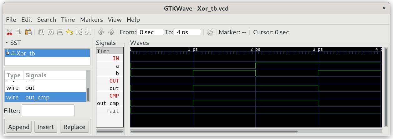
You can see four sections:
IN: the input signals (generated by the test bench)OUT: the output signals (generated by YOUR chip implementation)CMP: the output signals (generated by the test bench)Test: the fail signal. Goes high, when the test fails.
Your chip passes the test, when out=out_cmp and fail=0 over the whole test time.
iCE40HX1K.pcf
To upload the chip Xor onto your fpga board iCE40HX1K-EVB you need two additional files: top.v and iCE40HX1K.pcf (physical constraints file). The pyhiscal constraints file assigns every io-signal wire of the top level module top.v to physical pins of the fpga chip iCE40HX1K. Pin numbering can be checked by consulting the schematic iCE40HX1K-EVB in doc/iCE40HX1K-EVB_Rev_B.pdf.
#  physical constrain file
# assign io-pins to pin numbering of iCE40-HX1K on olimex board iCE40-HX1K-EVB
# compare to the schematic of the board and the datasheet of fpga

set_io BUT1 41    # BUT1
set_io BUT2 42    # BUT2

set_io LED1 40    # LED1
set_io LED2 51    # LED2
-
Now you can build and upload the chip
Xorto iCE40-HX1K-EVB with:$ apio clean $ apio build $ apio upload -
Press buttons BUT1 and BUT2 and see the result of your
Xorchip on LED1.
Attention: Due to pull up resistors at the buttons, the signals appear inverted:
| pin | function |
|---|---|
| LED1/2 | 0 led is off, 1 led is on |
| BUT1/2 | 0 button is pressed down, 1 button is released up |
Chips with note more than two in- and output signals can be uploaded and tested in real hardware: Nand, Not, Buffer, And, Or, Xor and DMux.