4.6 KiB
07 RTP
The special function register RTP memory mapped to addresses 4106 enables HACK to read bytes from the resistive touch panel controller chip AR1021 situated on MOD-LCD2.8RTP. The communication is protocol is SPI.
Attention: The specification of AR1200 requires, that SCK is inverted (compare 03_SPI/Readme.md with CPOL=1) and a slower transfer rate of max. 900kHz
Chip specification
| IN/OUT | wire | function |
|---|---|---|
| IN | in[7:0] | byte to be sent. |
| IN | load | =1 initiates the transmission |
| OUT | out[15] | =0 chip is busy, =0 ready |
| OUT | out[7:0] | received byte |
| IN | SDI | serial data in |
| OUT | SDO | serial data out |
| OUT | SCK | serial clock |
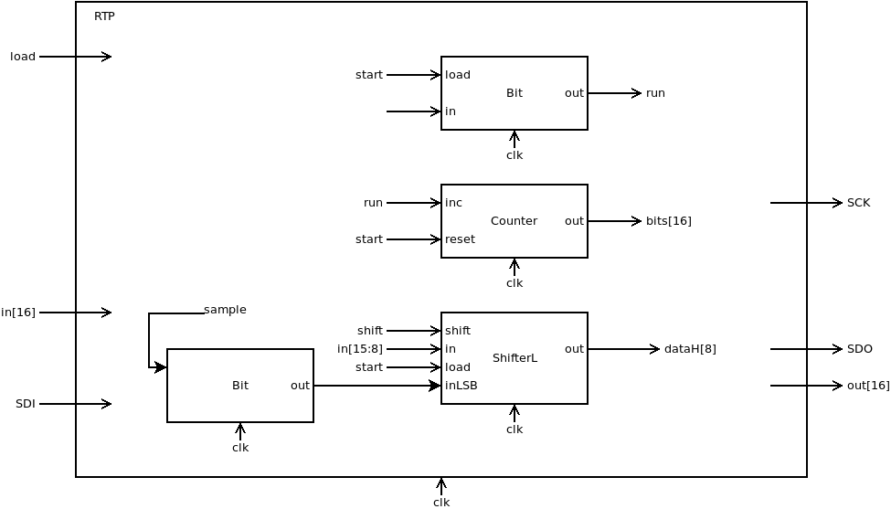
When load=1 transmission of byte in[7:0] is initiated. The byte is send to SDO bitwise together with 8 clock signals on SCK. At the same time RTP receives a byte at SDI. During transmission out[15] is 1. The transmission of a byte takes 256 clock cycles (32 cycles for each bit to achieve a slower transfer rate). Every 32 clock cycles one bit is shifted out. In the middle of each bit at counter number 31 the bit SDI is sampled. When transmission is completed out[15]=0 and RTP outputs the received byte to out[7:0].
Proposed Implementation
Use a Bit to store the state (0 = ready, 1 = busy) which is output to out[15]. Use a counter PC that counts from 0 to 511. Finally we need a BitShift8L. It will be loaded with the byte in[7:0] to be send. Use a Bit to sample the SDI line. After 8 bits are transmitted/received RTP cleares out[15] and outputs the received byte to in[7:0].
Attention: sample on rising edge of SCK and shift on falling edge of SCK.
Memory map
The special function register RTP is mapped to memory map of HACK according to:
| address | I/O device | R/W | function |
|---|---|---|---|
| 4106 | LCD | W | start transmittion of byte in[7:0] |
| 4106 | LCD | R | out[15]=1 busy, out[15]=0 idle, out[7:0] last received byte |
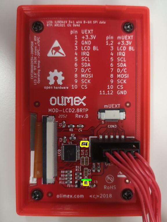
RTP in real hardware
The board MOD-LCD2.8RTP comes with a resistive touch panel controlled by a controller chip AR1021. MOD-LCD2.8RTP must be connected to iCE40HX1K-EVB with 3 more jumper wire cables according to iCE40HX1K-EVB.pcf (Compare with schematic iCE40HX1K_EVB and MOD-LCD2.8RTP_RevB.pdf.
set_io RTP_SDI 7        # PIO3_3A connected to pin 13 of GPIO1
set_io RTP_SDO 8        # PIO3_3B connected to pin 15 of GPIO1
set_io RTP_SCK 9        # PIO3_5A connected to pin 17 of GPIO1
| wire | iCE40HX1K-EVB (GPIO1) | MOD-LCD2.8RTP (UEXT) |
|---|---|---|
| +3.3V | 3 | +3.3V |
| GND | 4 | 2 GND |
| LCD_DCX | 5 | 7 D/C |
| LCD_SDO | 7 | 8 MOSI |
| LCD_SCK | 9 | 9 SCK |
| LCD_CSX | 11 | 10 CS |
| RTP_SDI | 13 | 4 IRQ/SDO (with solder jumper SJ3) |
| RTP_SDO | 15 | 6 SDA |
| RTP_SCK | 17 | 5 SCL |
Attention: To enable SPI communication on the RTP controller chip AR1021 we must modify two solder jumpers. (Compare with schematic of MOD-LCD2.8RTP together with Datasheet of AR1021).
-
Cut connection SJ1-GND with a sharp cutter knife. (green)
-
Connect SJ1 to +3.3V to activate SPI mode of AR1021 (yellow)
-
Connect SJ3 (UEXT pin4 with SDO) (yellow)
Project
-
Implement special function register
RTPand test with testbench:$ cd 07_RTP $ apio clean $ apio sim -
Compare output
OUTof special chipRTPwithCMP.
-
Add special function register
RTPtoHACKat memory addresses 4106 and upload to iCE40HX1K-EVB with bootloader boot.asm preloaded into ROM.$ cd ../05_GO $ make $ cd ../00_HACK $ apio clean $ apio upload -
Proceed to
07_Operating_Systemand implement the driver classTouch.jackthat sends command overRTPthe controller chip AR1021 on MOD-LCD2.8RTP