05 Computer Architecture
Build the HACK computer system consisting of the chips CPU, Memory, Clock25_Reset20, RAM and ROM. ROM uses a block ram structure (256 words) of iCE40HX1K and can be considered primitive. It can be preloaded with the instructions of the assembler programs implemented in 04_Machine_Language .
01 CPU
The CPU corresponds to the proposed implementation of nand2tetris course.
 Attention: In the original specification of HACK all C instruction have the binary form: 111xxxxxxxxxxxxx and A instruction have the form 0xxxxxxxxxxxxxxx. In order to use HACK with instruction memory ROM >32K (to play tetris), we will also interpret the machine language instructions starting with 000-110 as A-instructions, allowing the following jumps for all labels up to 56K!
@label
0;JMP
02 Memory
The chip Memory.v maps all addresses 0 - 0x0FFF to RAM and the addresses 0x1000-0x100F to the 16 special function registers used for memory mapped IO-Devices and debugging.
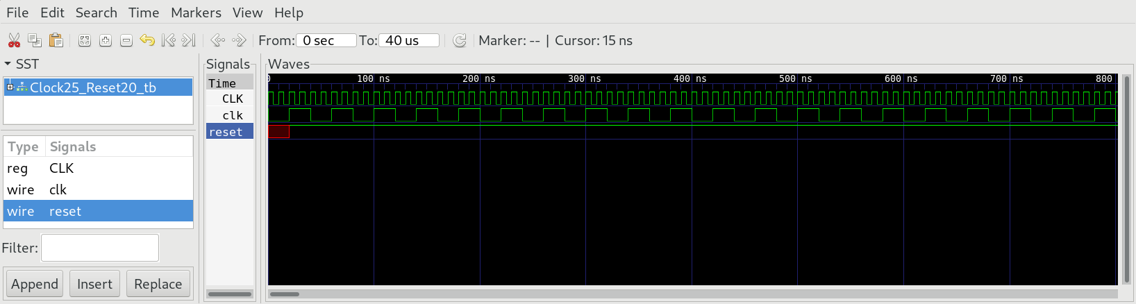
03 Clock25_Reset20
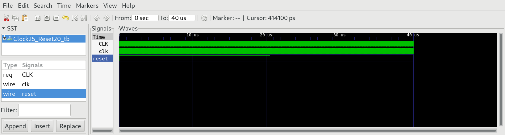
The 100 MHz (CLK) of the clock generator on the iCE40HX1K-EVB is to fast to drive our HACK design. Therefore we must scale down the external clock (CLK) of 100 MHz to the internal clock (clk) of 25Mhz using a counter PC .
HACK CPU needs a reset signal to have a proper start of the complete computer system. The fpga chip nees some time delay to preload the ROM with ROM.hack code. Therefore the reset signal at startup should have a minimal length of approximately 20us.
04 HACK
The chip HACK.v is the top level module, that connects to the outer world.

The signals wires CLK, RST, BUT[1:0] and LED[1:0] (by convention written in capital letters) connect to the outer pins of the fpga chip iCE40HX1K according to the file iCE40HX1K.pcf. The board iCE40-HX1K-EVB comes with a clock generator of 100 MHz, two buttons and two leds connected to FPGA (refer to datasheets/iCE40HX1K-EVB).
| wire | iCE40HX1K (FPGA) | board iCE40HX1K-EVB |
|---|---|---|
| CLK | 15 | 100 Mhz clock generator |
| BUT[0] | 41 | BUT1 |
| BUT[1] | 42 | BUT2 |
| LED[0] | 40 | LED1 |
| LED[1] | 51 | LED2 |
To add IO capability we add 7 more special function registers mapped to the following addresses:
| address | I/O dev | function |
|---|---|---|
| 0 - 3839 | RAM | |
| 4096 | LED | 0 = led off, 1 = led on |
| 4097 | BUT | 0 = button pressed "down", 1 = button released |
| 4098 - 4106 | reserved for IO devices (see. project 06_IO_Devices) | |
| 4107 - 4111 | DEBUG | used for debugging |
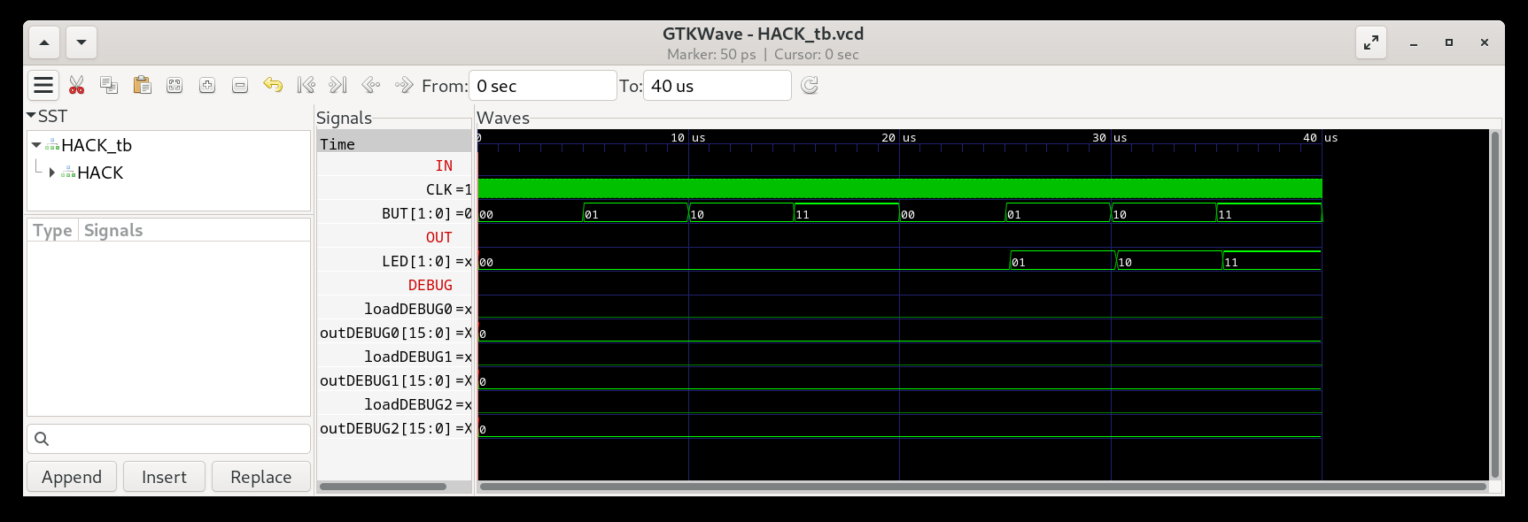
The HACK simulation needs a valid file ROM.hack (created in project 04_Machine_Language) with the machine language instructions to perform.
The test bench of 04_HACK will:
- occasionally press the user buttons BUT1/2
- show the result of LED1/2
- show the content of DEBUG0-DEBUG5
Project
-
Implement the chips
CPU,MemoryandClock25__Reset20and simulate with the corresponding test benches:$ cd 0X_<chipname> $ apio clean $ apio sim -
Check the frequency of the internal clk signal to be 25MHz. So one clock cylce takes 40us.
-
Check the reset signal of HACK. You should see a reset signal of approximately 20 us.


-
Implement
HACKand test withleds.asm:$ cd ../04_Machine_Language $ make leds $ cd ../05_Computer_Architecture/04_HACK $ apio clean $ apio sim -
Check, if LEDs change state accoring to BUT:
-
Test
HACKwithmult.asm.$ cd ../04_Machine_Language $ make mult $ cd ../05_Computer_Architecture/04_HACK $ apio clean $ apio sim -
You should see the result 715 of the multiplication 13*55 in the debug register
DEBUG2! You can change the number format to decimal.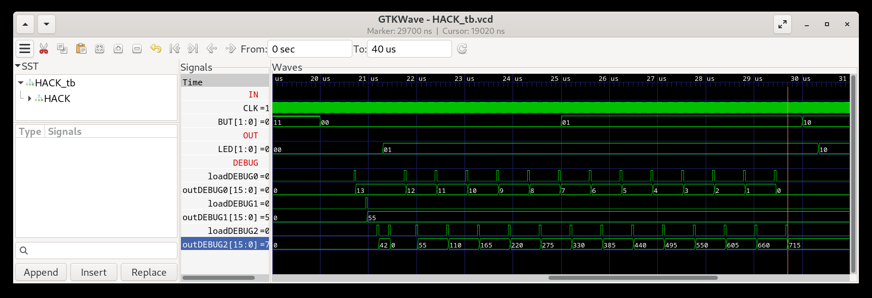
-
finally upload the complete HACK design with
leds.asmpreloaded into instruction ROM and run in real hardware!$ cd ../04_Machine_Language/01_leds $ make $ cd ../05_Computer_Architecture/04_HACK $ apio clean $ apio build $ apio upload -
press the user buttons BUT1/BUT2 and see if the LED change pattern accordingly.
-
Repeat the test with the second machine language programm
mult.asm.


Attention: remember to run apio clean, after changing the file ROM.hack!