06 LCD
The special function register LCD memory mapped to addresses 4104 and 4105 enables HACK to write bytes to the LCD controller chip ILI9341V situated on MOD-LCD2.8RTP. The communication protocol is SPI with one additional wire DCX. The protocol defines transmission of 8 bit commands with DCX = 0 followed data with DCX=1. Data packets can have any length depending on the launched command.
Chip specification
| IN/OUT | wire | function |
|---|---|---|
| IN | in[7:0] | byte to be sent. |
| IN | in[8] | =0 send byte and set CSX low |
| IN | in[8] | =1 pull CSX high without sending byte |
| IN | in[9] | value of DCX when transmitting a byte. |
| IN | load | initiates the transmission of a byte, when in[8]=0 |
| IN | load16 | initiates the transmission of 16 bit in[15:0] |
| OUT | out[15] | =0 chip is busy, =0 ready |
| OUT | DCX | =0 command, =1 data |
| OUT | SDO | serial data out |
| OUT | SCK | serial clock |
| OUT | CSX | chip select not |
The special function register LCD communicates with ILI9341V LCD controller over 4 wire SPI.
When load=1 and in[8]=0 transmission of byte in[7:0] is initiated. CSX is goes low (and stays low even when transmission is completed). DCX is set to in[9]. The byte in[7:0] is send to SDO bitwise together with 8 clock signals on SCK. During transmission out[15] is 1. After 16 clock cycles transmission is completed and out[15] is set to 0.
When load=1 and in[8]=1 CSX goes high and DCX=in[9] without transmission of any bit.
When load16=1 transmission of word in[15:0] is initiated. CSX is goes low (and stays low even when transmission is completed). DCX is set to 1 (data). After 32 clock cycles transmission is completed and out[15] is set to 0.
Proposed Implementation
Use a Bit to store the state (0 = ready, 1 = busy) which is output to out[15]. Another two Bit store the state of DCX and CSX. Use a counter PC to count from 0 to 15 or 31 according to load/load16. Finally we need two connected BitShift8L. They will be loaded with the byte in[7:0] or the word in[15:0] to be send. After 8/16 bits are transmitted the module cleares out[15].

Memory map
The special function register LCD is mapped to memory map of HACK according to:
| address | I/O device | R/W | function |
|---|---|---|---|
| 4104 | LCD | W | start transmittion of byte in[7:0] |
| 4105 | LCD | W | start transmittion of word in[15:0] |
| 4104/4105 | LCD | R | out[15]=1 busy, out[15]=0 idle |
LCD in real hardware
The board MO-LCD2.8RTP comes with a 2.8 inch LCD screen controlled by a controller chip ILI8341V. MOD-LCD2.8RTP must be connected to iCE40HX1K-EVB with 6 jumper wire cables: +3.3V, GND plus 4 data wires according to iCE40HX1K-EVB.pcf (Compare with schematic iCE40HX1K_EVB and MOD-LCD2.8RTP_RevB.pdf.
set_io LCD_DCX 1        # PIO3_1A connected to pin 5 of GPIO1
set_io LCD_SDO 2        # PIO3_1B connected to pin 7 of GPIO1
set_io LCD_SCK 3        # PIO3_2A connected to pin 9 of GPIO1
set_io LCD_CSX 4        # PIO3_2B connected to pin 11 of GPIO1
| wire | iCE40HX1K-EVB (GPIO1) | MOD-LCD2.8RTP (UEXT) |
|---|---|---|
| +3.3V | 3 | 1 +3.3V |
| GND | 4 | 2 GND |
| LCD_DCX | 5 | 7 D/C |
| LCD_SDO | 7 | 8 MOSI |
| LCD_SCK | 9 | 9 SCK |
| LCD_CSX | 11 | 11 CS |
Project
-
Implement
LCD.vand test with testbench:$ cd 06_LCD $ apio clean $ apio sim -
Compare output
OUTof special chipLCDwithCMP.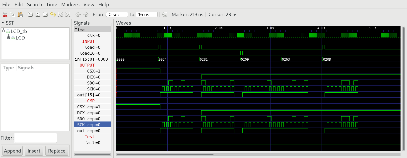
-
Add special function register
LCDtoHACKat memory addresses 4104/4105 and upload to iCE40HX1K-EVB with the bootloader boot.asm preloaded into ROM$ cd ../05_GO $ make $ cd ../00_HACK $ apio clean $ apio upload -
Proceed to
07_Operating_Systemand implement the driver classScreen.jackthat sends command overLCDthe controller chip ILI9341V on MOD-LCD2.8RTP
