04 SRAM
The evaluation board iCE40HX1K-EVB includes an 512kbyte static ram chip K6R4016V1D. The SRAM chip connects to iCE40HX1K with 37 wires;
- SRAM_ADDR 18 bit
- SRAM_DATA 16 bit (bidiretional inout)
- SRAM_CSX (chip select not)
- SRAM_OEX (output enable not)
- SRAM_WEX (write enable not)
To read and write to the SRAM chip we will add two special function register to HACK:
-
SRAM_A is a 16 bit register mapped at memory location 4104. SRAM_ADDR controls the 16 lower bits of the 18 bit address bus. The two most significant bits are allways 0, so we can only access 64k x 16 bit words of SRAM chip.
-
SRAM_D is a special function register mapped at memory location 4105. SRAM_D controls the bidirectional data bus and the control wires CSX, OEX and WEX.
Note: the 16 bit data bus is bidirectional and has therefore to be connected over a tristate buffer. This is done with InOut.v which is considered primitive and must not be implemented.
Chip specification SRAM_A
SRAM_A is a simple Register that stores the lower 16 bit of the 18 bit address of the SRAM chip.
Chip specification SRAM_D
| IN/OUT | wire | function |
|---|---|---|
| IN | clk | system clock (25MHz) |
| IN | load | initiate a write operation |
| IN | in[15:0] | data to write to SRAM |
| OUT | out[15:0] | data read from SRAM |
| INOUT | SRAM_DATA[15:0] | bidirectional data bus |
| OUT | SRAM_CSX | chip select not |
| OUT | SRAM_OEX | output enable not |
| OUT | SRAM_WEX | write enable not |
When load[t]=1 transmission of word in[15:0] is initiated. The word is send to SRAM over the bidirectional wires SRAM_DATA (direction out) and a write pulse will be triggered for one cycle at t+1:
-
SRAM_OEX=1
-
SRAM_WEX=0
When load=0 SRAM_DATA will be used as input and the data of the SRAM chip will be presented at out[15:0]
-
SRAM_OEX=0
-
SRAM_WEX=1
SRAM_CSX can be set to low all the time.
Proposed Implementation ADDR_A
Use a Register to store the lower 16 bit of SRAM_ADDR (The two most significant bits are hardwired to 0).
Proposed Implementation ADDR_D
Use a DFF to delay the load signal. Use a Register to store the data in[15:0] to be stored. Use a tristate buffer InOut.v to control the direction of the bidirectional SRAM_DATA data bus.
Memory map
The special function register SRAM_A and SRAM_D are mapped to memory map of HACK according to:
| address | I/O device | R/W | function |
|---|---|---|---|
| 4101 | SRAM_A | R | address of SRAM |
| 4102 | SRAM_D | R | read data from SRAM |
| 4102 | SRAM_D | W | initiate a write cylce to SRAM |
buffer.asm
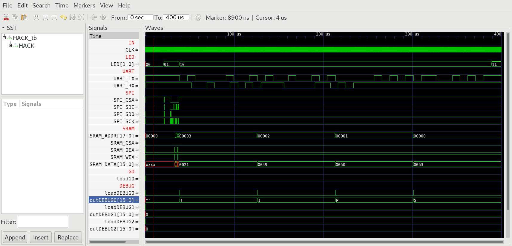
To test HACK with SRAM we need a little machine language programm buffer.asm, which reads the first four bytes of an ASCII file previosuly stored to the SPI flash memory chip W25Q16BV of iCE40HX1K-EVB, starting at address 0x040000 (256k) and stores the four bytes to SRAM. Finally we read the four bytes from SRAM and write them to UART.
SRAM in real hardware
The board iCE40HX1K-EVB comes with a static ram chip K6R4016V1D. The chip is already connected to iCE40HX1K according iCE40HX1K-EVB.pcf (Compare with schematic iCE40HX1K_EVB.
set_io SRAM_ADDR[0] 79 # SA0
set_io SRAM_ADDR[1] 80 # SA1
set_io SRAM_ADDR[2] 81 # SA2
set_io SRAM_ADDR[3] 82 # SA3
set_io SRAM_ADDR[4] 83 # SA4
set_io SRAM_ADDR[5] 85 # SA5
set_io SRAM_ADDR[6] 86 # SA6
set_io SRAM_ADDR[7] 87 # SA7
set_io SRAM_ADDR[8] 89 # SA8
set_io SRAM_ADDR[9] 90 # SA9
set_io SRAM_ADDR[10] 91 # SA10
set_io SRAM_ADDR[11] 93 # SA11
set_io SRAM_ADDR[12] 94 # SA12
set_io SRAM_ADDR[13] 95 # SA13
set_io SRAM_ADDR[14] 96 # SA14
set_io SRAM_ADDR[15] 97 # SA15
set_io SRAM_ADDR[16] 99 # SA16
set_io SRAM_ADDR[17] 100 # SA17
set_io SRAM_CSX 78 # SRAM_#CS
set_io SRAM_OEX 74 # SRAM_#OE
set_io SRAM_WEX 73 # SRAM_#WE
set_io SRAM_DATA[0] 62 # SD0
set_io SRAM_DATA[1] 63 # SD1
set_io SRAM_DATA[2] 64 # SD2
set_io SRAM_DATA[3] 65 # SD3
set_io SRAM_DATA[4] 66 # SD4
set_io SRAM_DATA[5] 68 # SD5
set_io SRAM_DATA[6] 69 # SD6
set_io SRAM_DATA[7] 71 # SD7
set_io SRAM_DATA[8] 72 # SD8
set_io SRAM_DATA[9] 60 # SD9
set_io SRAM_DATA[10] 59 # SD10
set_io SRAM_DATA[11] 57 # SD11
set_io SRAM_DATA[12] 56 # SD12
set_io SRAM_DATA[13] 54 # SD13
set_io SRAM_DATA[14] 53 # SD14
set_io SRAM_DATA[15] 52 # SD15
Project
-
Implement
SRAM_D.vand simulate with testbench:$ cd 04_SRAM_D $ apio clean $ apio sim -
Compare output of your chip
OUTwithCMP.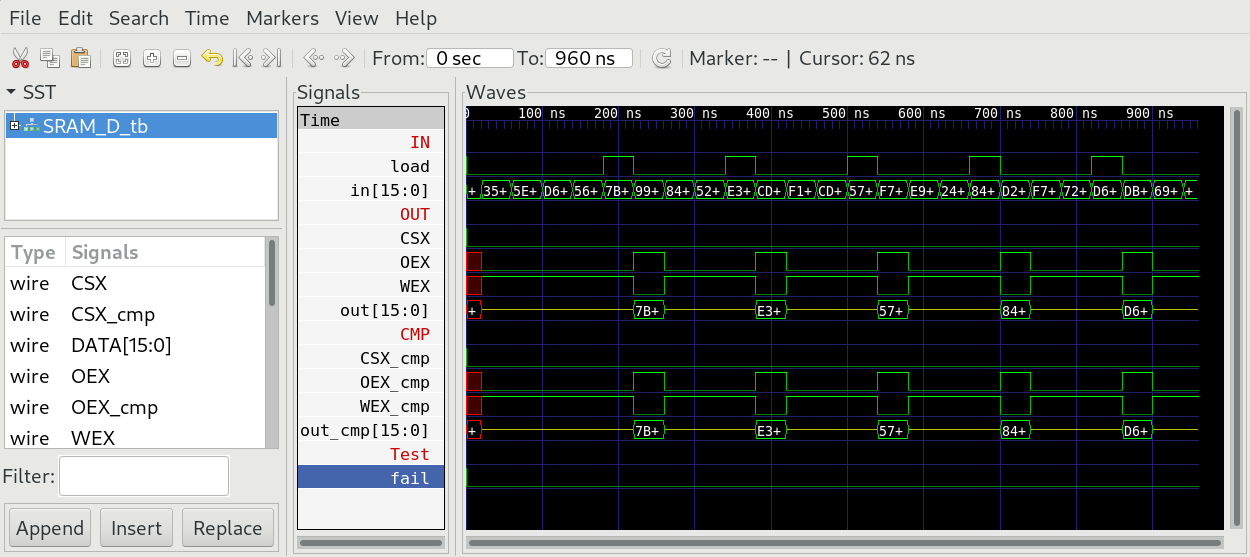
-
Edit
HACK.vand add aRegisterfor SRAM_A memory mapped to 4101. -
Edit
HACK.vand add a special function registerSRAM_Dto memory address 4102. -
Implement
buffer.asmand test with the testbench:$ cd 04_SRAM_D $ make $ cd ../00_HACK $ apio clean $ apio sim -
Check the SRAM wires of the simulation and look for the storing of "SPI!" (which was preloaded in SPI chip at memory address 0x040000 of the testbench).
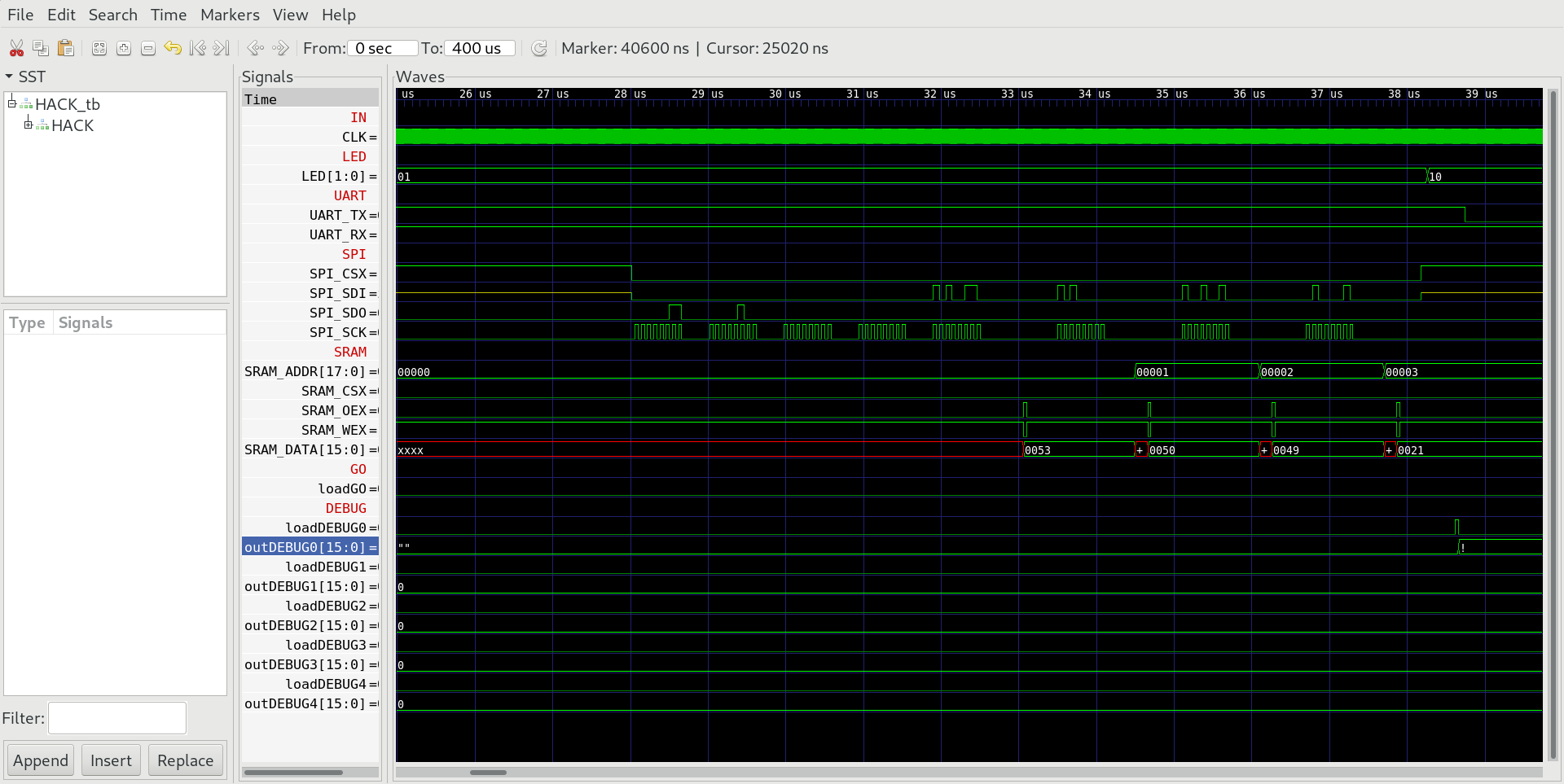
-
Check the output at UART_TX in the long run. You should see the string "SPI!" output to UART_TX:
-
preload the SPI memory chip with some text file at address 0x040000.
-
build and upload HACK with
buffer.asmin ROM.BIN to iCE40HX1K-EVB.


-
press reset button on iCE40HX1K-EVB and see if wou can receive the preloaded text file on your Computer.
$ echo SPI! > spi.txt
$ iceprogduino -o 256k -w spi.txt
$ cd 04_SRAM_D
$ make
$ cd ../00_HACK
$ apio clean
$ apio upload
$ tio /dev/ttyACM0